
Issue # 59
Special PDM Issue April, 1988
Scanned, and OCR'ed by Bob "Bacon" Bruhns, WA3WDR
![]()
FCC Proposes Sweeping Changes to Ham Rules
No longer in the "vacuum tube age", commissioner says
In a public meeting on March 24, the FCC decided to issue a Notice of Proposed Rulemaking to streamline and clarify Part 97 of its rules governing amateur radio. Docket PR 88-139 is entitled "Reorganization and Deregulation of Part 97 of the Rules Governing the Amateur Radio Service." John B. Johnston, W3BE, Chief of the FCC's Personal Radio Branch, said that the deregulation was "more in terms of dropping out obsolete and repetitious rules" rather than new regulations. It was Johnston who rewrote the rules. Ralph Haller, N4RH, Chief, Private Radio Bureau "had a lot of personal involvement in it," as did Ray Kowalski, ex-Chief, Special Services Division before he left. Johnston said they hope to have the docket out by Dayton. Johnston is scheduled to address the HamVention and it appears his main subject will be the new Part 97.
At the March 24 Commissioner's meeting, Personal Radio Branch attorney John Borkowski delivered the formal presentation to Commissioners Dennis Patrick (chairman), James Quello, and Patricia Dennis. Borkowski stated, "This item proposes to reduce the total body of Amateur Radio Service rules by almost forty percent, by deleting those rules that are unnecessary, obsolete, or redundant. Just as important, this proposal would reorganize Part 97 to account for the tremendous advances in technology, and concomitant changes in operating practices... The current rules have not undergone a major reorganization since 1951. They have evolved one at a time, in response to the introduction of new technologies. They are based upon telegraphy and AM telephony operating practices. (emphasis ours -Ed.) The proposed reorganized rules before you would more readily accommodate current and future technologies and operations. They will promote a regulatory environment that fosters maximum operator flexibility, and innovative technological uses and experimentation... (the Docket) does propose certain limited substantive changes. They are in the areas of permissible emission type, and codification of certain policies not currently specified in the rules."
In the discussion that followed the presentation, Commissioner Dennis stated, "...It recognizes that we're no longer in the vacuum tube age, and that was the early '50s, and we recognize that we're now in the solid-state micro-chip age."
The NPRM proposes to simplify the system of emission designators to be used by Amateur Radio. With "considerable help" from the ARRL's Paul Rinaldo, W4RI (Editor of QST), the authors of the Docket came up with nine general emission terms that are already familiar to amateur operators, and categorized all the present ITU designators under those nine terms. They are: (1) CW: single channel amplitude-shift-keyed telegraphy in International Morse Code for aural or automatic reception. (2) MCW: single channel modulated tone telegraphy emissions in International Morse Code for aural or automatic reception. (3) PHONE: telephony/voice emissions. (4) IMAGE: single channel emissions for television and facsimile, etc. (5) RTTY: single channel emissions for narrow-band direct printing. (6) DATA: digital data including packet. (7) PULSE: pulse emissions. (8) SS: Spread Spectrum emissions. (9) TEST: emissions containing no modulation or information used for on air transmitter adjustment, two-tone amplifier linearity testing, antenna measurement, direction finding, etc.
Comments on PR Docket 88-139 will be due on or before August 31, 1988, with replies due on or before October 31, 1988.
We wish to thank the W5YI Report newsletter for providing the above information, and giving blanket permission to reproduce it. The Docket is not yet available to the public at this writing, but should be released about April 15. We plan to print pertinent extracts from the Docket as space permits next issue.
Pulse Duration Modulators
by Stephen Cloutier KA1SI
This article describes the operation, and presents some practical circuit details of Pulse Duration Modulators. Over the years I have designed and built several AM transmitters using the PDM system. If we have spoken on 75 or 160M in the last year then you have probably heard one of my PDM transmitters, since it is the only transmitter I have on the air!
SCOPE OF THIS ARTICLE
I will be describing one variation of a PDM system. Other circuit topologies are possible. The one I will describe is the simplest and most straight-forward variation that I have found. This article presents information to allow someone with a reasonable knowledge of radio and electronics to understand how the PDM system works, and to design and build a transmitter using the PDM system. Where ever possible, standard components are used. There are some components necessary for the construction of a PDM transmitter which are not commercially available. Construction details for these components are included. To properly test a PDM system, you will need access to a 20 MHz or better oscilloscope, and an audio signal generator.
The circuits shown are functionally complete. However, to avoid cluttering the diagrams any more than necessary, the usual bypass capacitors at each power lead of each IC have been eliminated, along with the power leads themselves. Since this is standard practice, it is assumed that the builder would include bypasses and such even if they are not shown in a diagram. Since the Pulse Duration Modulator uses non-resonant, wide band high frequency RF for its operation, care must be taken to avoid intercircuit coupling, oscillations, ringing and other common problems which plague poor circuit layouts.
PDM TRANSMITTER THEORY OF OPERATION - How and why does it work
NOTE: A Pulse Duration MODULATOR differs, in the strict sense of the word, from Pulse Duration MODULATION, the latter generally involving the transmission of pulses directly via a carrier, or transmitting RF pulses of varying duration. In this discussion, the modulator uses Pulse Duration Modulation internally, however, the pulses are removed and the output converted to modulated, standard audio-modulated DC before application to the modulated RF stage. -end Note.
The PDM transmitter consists of a High-level modulated, standard class C amplifier, and in most applications, a very efficient series modulator. A series modulator is just what its name implies - a device in series with the RF amplifier and the power supply.
As far as audio quality is concerned, the series modulator is probably the best high-level modulator circuit that you can use. It uses no transformers, is DC coupled (very important if you use sophisticated audio processing techniques) and is fairly easy to implement. The disadvantage of the class A series modulator is, of course, the low efficiency of the system. The PDM system has all the advantages of the series modulator (no transformers, DC coupled, etc) but does not suffer from the tremendous inefficiency and power loss of the class A amplifier.
In a PDM system, the modulator device or devices (tubes, FETS, transistors, etc) are switched between saturation (fully turned on - minimum voltage drop across device) and cutoff (no current flow through device) at a frequency at least 3 or 4 times the highest audio frequency we wish to modulate. The switching frequency is then filtered out so that only original modulating signal remains. Since the modulator devices are always operating at either saturation (very low voltage drop) or cutoff (no current), the power dissipated in the modulator is very low, and therefore the efficiency is very high.
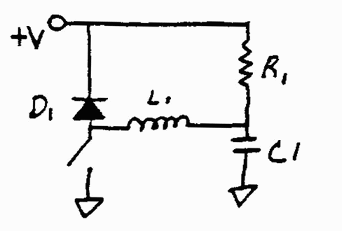
Let us now develop a basic Pulse Duration modulator. Since all devices in such a modulator are acting like switches, we will use an actual switch to illustrate how these modulators work. In practice, of course, a FET, tube, or transistor is used as the modulator. Consider the basic circuit shown in figure A:
When the switch is closed, a current will begin to flow in inductor L1 through the load resistor R1, and from C1 as C1 begins to discharge. The current flowing in L1 causes energy to be stored in the magnetic field within the inductor. If the switch is now opened, the current flow through L1 will immediately stop. The magnetic field within the inductor will quickly collapse, producing a current flow in the opposite direction, and therefore a reverse voltage across the inductor. The voltage will quickly rise, until it reaches the power supply voltage. At that point, diode D1 will begin to conduct, and will not allow the voltage to rise any higher. The current developed by the reverse voltage will be conducted through the diode back to the power supply. When the switch is turned back on, the cycle repeats - off, on, off, on, etc... The period of time that the switch is closed is the modulator "on-time".
The voltage (and current) at the output of the filter is directly related to the ratio of modulator on-time vs off-time. Since the voltage at the output of the filter is based on the mathematical average of the pulses appearing at the input of the filter, an expression can be derived which is useful in predicting modulator operation:
| Vout = ((t1 * V1) + (t2 * V2)) / (t1 + t2) |
where: Vout is the voltage measured at the output of the filter, V1 is one of the voltages in the switching waveform (either high or low), t1 is the time (in any unit) that the switching waveform remains at V1. V2 is the other voltage in the switching waveform, and t2 is the time (in the same units as t1) that the voltage remained at V2. The expression (t1 + t2) is actually the switching rate of the modulator.
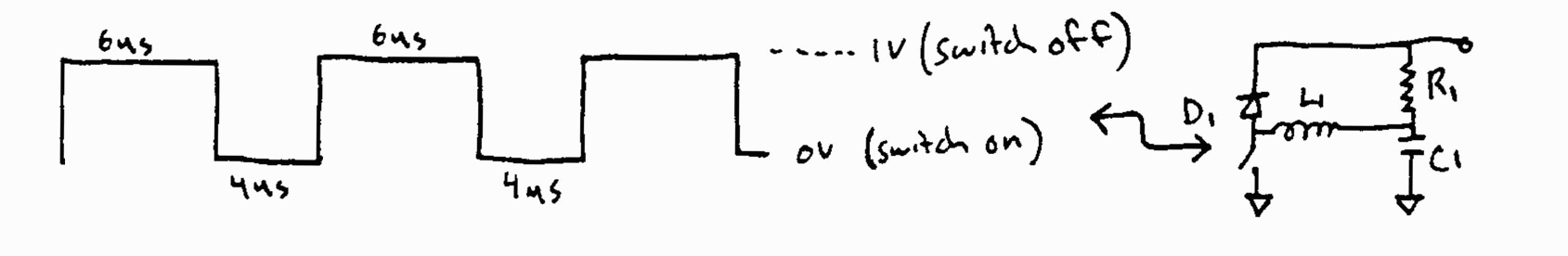
In a typical example, a modulator is operating such that the on-time is 4uS and the off time is 6uS. The switching waveform produced by the circuit in figure A would look like this:
Click to see switching waveform
The 4uS on time, we'll call t1. The 6uS off time is t2. If the values are substituted into the expression:
| Vout = ((4uS * 0V) + (6uS * 1V)) / (4uS + 6uS) = 6uS-V/10uS = .6V |
This is the voltage measured at the output of the filter, with respect to ground. The voltage ACROSS the load is, of course, .4V.
If the on-time is increased to, let's say, 7uS, the off-time will then be 3uS, since the switching rate is always the same, in this case 10uS. If the output voltage is now calculated, we will get .3V at the output of the filter, which causes the voltage across the load to increase to .7V.
The on-time is generally called the pulse-width, which is where the name for this type of modulator is derived. Notice that we have controlled the voltage across the load by simply varying the pulse width. That is how the modulator works - controlling the average voltage (pulses filtered out) across the load by changing duty cycle (pulse width or on time) of the modulator.
Any active device, such as a FET, tube, or transistor can be used as the modulator. The diode can be a tube, or fast-recovery solid-state diode. The load resistor R1 represents the final RF amplifier. This comprises most of the Pulse Duration Modulator. In a typical operation, the voltage across the RF amplifier is generally set to be 40% of the total supply voltage. The pulse waveform is set up so that, at carrier (no modulation) the modulator device is on for 40% of the total time, and off for 60% of the total time. With this arrangement, the amplifier could be modulated up to 150% positive.
Any circuit which generates variable width pulses can be used as the basis of a pulse duration modulator. The modulator could use devices in push pull connected to a transformer whose output is then rectified, multiple modulator devices operating in different phases... etc. The design of these systems is left to the imagination of the reader - and hopefully - future articles.
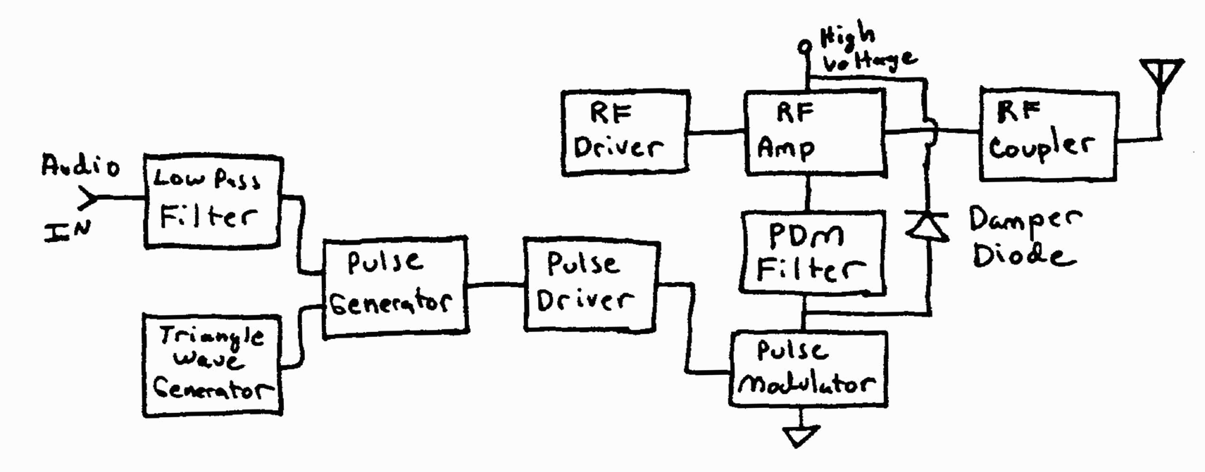
DESIGN OF THE BASIC SYSTEM
Figure B shows a functional diagram of a PDM transmitter. Each functional component will be discussed separately.
Pulse duration modulation generators
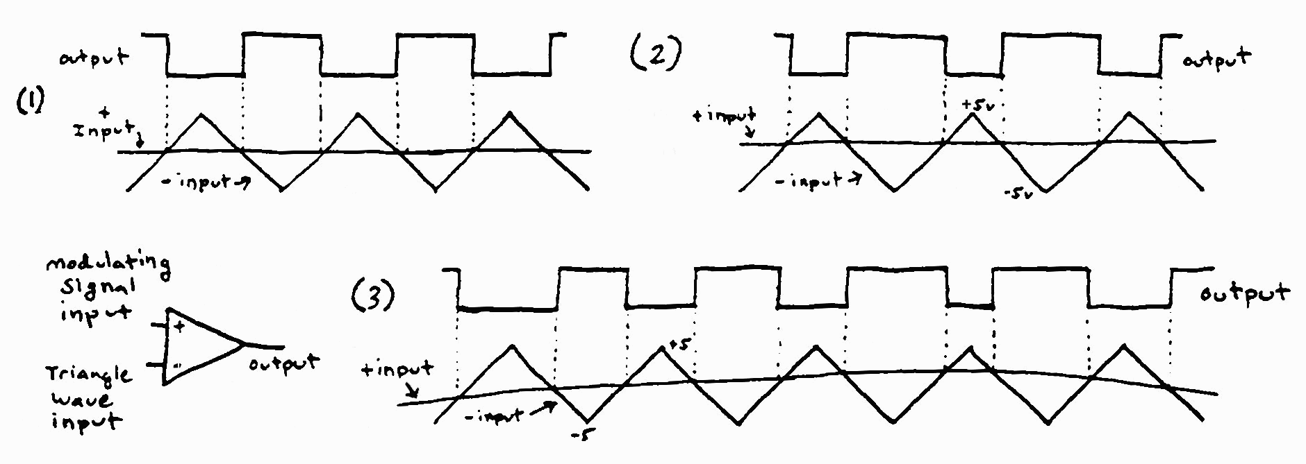
A PDM Generator is any circuit which produces a pulse whose width is proportional to the input amplitude of the applied signal. A simple method of producing such a signal uses a differential comparator and a triangle wave generator. A differential comparator generates either a high or low output (digital signal), based on the voltage difference between 2 input signals. The triangle wave is fed into one input, and the modulating signal is fed to the other input. Referring to figure C, the triangle wave generator is fed to the "-" input of the comparator. The audio to the "+" input. The comparator works as follows: When the level of the "+" input is higher than the level of the "-" input, the comparator generates a logic 1 (high) output. When the "-" input is higher than the "+" input, a logic 0 (low) is generated. Let us assume, for the moment, that the triangle generator produces a 10V peak-to-peak output. The "-" input of the comparator is, therefore, varying between +5 and -5 volts (10v P-P). If the signal fed to the "+" input is 0, the output of the comparator will be an exact 50% duty cycle square wave. This is illustrated in figure C(1). Let us now connect a +1 volt DC source to the "+" input of the comparator. If no other factors change, the output from the comparator will very closely resemble the signal shown in figure C(2). The reason that the 1 (high) pulse is longer than the 0 (low) pulse is that the portion of the triangle wave which is less than 1 volt, and therefore makes the "+" input greater than the "-" input, is wider than the portion which is greater than 1 volt. If now, rather than connecting a DC signal to the "+" input, we connect a sine wave to the "+" input, we will produce varying width pulses whose width depends on the width of the triangle wave for the time where the "+" input is greater than the input. The pulse train shown in figure C(3) shows the variable width pulses produced by a sine wave input.
As we mentioned earlier, the output from the comparator is a digital signal - that is, the signal has only 2 possible states, high and low. The information (modulation), rather than appearing as an amplitude change, as in the input, appears as a change in the ratio between the times that the signal is high and low. The amount of change is directly related to the amplitude of the input signal, and the rate of change is the frequency of the input signal. One of the nicest aspects of pulse duration signals is that they can be amplified without regard to amplitude linearity - in fact, the best amplifiers for this application are amplifiers designed to operate in the saturation/cutoff, or switch mode.
The triangle wave generator must produce perfectly linear triangles if good modulation linearity is to be expected. The distortion characteristic of the transmitter is determined more by the design of the triangle wave generator than any other part of the modulator. Care must be taken to ensure that the output of the triangle generator is unaffected by the input signal, power line variations, RF or any other outside factor. The tips of the triangles should be sharp and pointy. If they are rounded, nonlinearity and distortion of the modulating signal will occur. The sides of the triangles need not be identical in length. Often, the output will more resemble a sawtooth than a triangle. This is OK as long as both sides are perfectly straight and linear. A good circuit for a triangle wave generator will be presented later.
The switching frequency (determined by the frequency of the triangle wave generator) should be at least 4 times as high as the highest audio frequency you want to modulate. This ensures adequate resolution of the high frequencies and reduces the possibility of aliasing, a type of distortion caused by the mixing of the switching frequency and the input signal. It also makes design of the output filter easier. However, if the switching frequency is too high, the pulse generator and amplifier design will become difficult, due to the higher bandwidth required for high switching frequencies. Switching frequencies of between 50kHz and 100kHz are used in most Pulse Duration Modulators with 70kHz being very popular with broadcast equipment designers.
Low Pass Filter
A low-pass filter should be used ahead of any PDM generator. This filter prevents any harmonics or other signals near to the switching frequency from reaching the comparator. If the filter were not present, high frequency audio harmonics or other signals may mix with the switching frequency to produce unwanted signals in the audio range. This type of distortion is known as aliasing. It is very noticeable, but easy to prevent with a proper input filter.
Pulse Amplifier
The pulse amplifier/driver is used to drive the final devices used in modulator. It supplies whatever drive is necessary for the particular devices used. An extremely important consideration in designing the pulse amplifier/driver is the bandwidth, or 'speed' of the circuit. Inadequate amplifier bandwidth will generally cause distortion to appear at the extremes of modulation, both positive and negative, but is much more of a problem on the negative peak. If the rise and fall time of the pulse is too long, very short pulses will be stretched out, or may disappear entirely. If you want your pulse duration modulator to be able to modulate your transmitter up to 99% negative, without distortion, then the pulse amplifier should be capable of passing a pulse which is 1/100th of the total period of the switching waveform. With switching frequencies below 100kHz, this is not terribly difficult to achieve, as we will see later.
Output filter
The output filter usually consists of a multi-section L-C filter which must be specifically designed for the particular transmitter in which it is to be used. The number of filter sections will depend on the switching frequency, and how much attenuation of the switching frequency is desired. It is highly recommended that the switching frequency be attenuated at least 60dB or more. If your signal is 60dB over s9, and you only have 40dB of filtering, you will produce 2 sidebands, 20dB over s9 at plus and minus the switching frequency!! If you are building a powerful transmitter, more than 60dB of filtering should be used. There are many different types of filter arrangements which will work with these modulators. I will describe the method I use to design the filters in my transmitters. It is reasonably straight forward, and uses filter information which is available in the ARRL handbook (can you believe that?!!! The ARRL actually put something in the handbook relating to AM, and they didn't even know it!!!), and other common sources.
The filter I use is a constant K low-pass filter. It is a 4 element filter, using 2 inductors and 2 capacitors. The corner (the frequency at which the filter begins attenuation) is set at 12.5kHz. I use a switching frequency of 88kHz. A 4 element filter with the corner set at 12.5kHz should attenuate the 88kHz switching frequency more than 60dB. Each reactive element in the filter should, theoretically, give 6dB of attenuation per octave above the corner frequency. Design of the filter is dependent on basically 3 things: the impedance that the filter operates at, the corner frequency of the filter, and the number of elements in the filter. The load on the output of the filter is the DC resistance of the RF amplifier. I designed the filter to have the same input and output impedance. This approach has always given excellent results.
It is possible to write an entire article on the filter design alone. Space does not permit that, however. The newer ARRL handbook, West Coast Handbook, and many other sources have filter tables which will aid in designing the filter. The design of the filter is not particularly difficult when using the filter tables. In practice, there is considerable room for slop, in the filter design - so it's not quite as critical as it may seem to get the "exact" values for all the components.
PRACTICAL PDM TRANSMITTERS - making it work in the real world
This section presents practical details for building a PDM transmitter. I have included circuits for most sections of the transmitter. Please keep in mind that these circuits are EXAMPLES of how to implement a particular function. Your implementation may use some of these circuits, or parts of them. The circuit examples presented assume that the modulator is operated at DC ground, and that the RF amplifier is designed to be modulated in the cathode. However, there is no technical reason why the cathode of the RF amplifier cannot be grounded, and the modulation applied to the plate. The operating principals are the same for either system. The implementation will however, be quite different.
Triangle wave generator
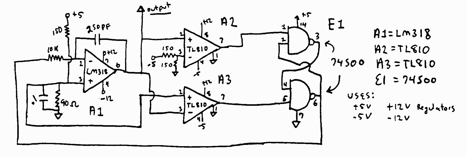
The triangle wave generator MUST be of good quality. As explained earlier, the distortion characteristics of the transmitter are directly determined by the quality of the triangle generator. I use an R/S flip flop followed by an active integrator and 2 comparators to generate the triangle waves for input to the comparator. The triangle wave generator has its own voltage regulators to improve the isolation from other circuits. It is of the utmost importance that the triangle generator and all other low level circuits in a PDM transmitter be completely isolated from RF and other circuits in the system. If the frequency, amplitude or waveshape of the triangle generator is affected by external events, distortion of the modulated signal will result. The circuit shown will generate a triangle wave around 70kHz. Referring to the figure D, Op amp A1 is set up as an integrator. A pre-bias voltage is fed to the + input of A1 so that the logic low produced by flip-flop E1 (usually 1 volt or thereabouts) will cause the integrator output to go positive. The integrator output is fed to one input of 2 comparators A2 and A3 which will switch alternately when the output rises above or below the DC voltages fed to their other inputs. The comparator outputs trigger the wired R/S flip flop, which in turn drives the integrator. The main frequency determining components are R1 and C1. As always, the output of the generator should be carefully checked on an oscilloscope before any use is attempted. Figure D shows the triangle wave generator:
Negative Peak Limiter, Filter and Pulse Generator
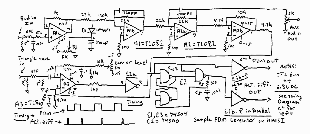
The circuit shown in figure E shows a sample pulse generator. The circuit contains the input circuitry including a negative peak limiter, filter, and carrier set. Three outputs are provided: a standard PDM output, an "active differentiator" output which produces a 50uS pulse on the falling edge of the standard PDM output, and an auxiliary analog output for use by the high level driver. The pulse outputs are 5 Volt outputs. The impedance of the outputs is very low, and will drive the gates of power MOSFETs directly. Short leads between the outputs and the gates of MOSFETs are very important.
Referring to figure E, audio is fed to buffer amplifier A1a, which drives the negative peak limiter D1. Resistor R1 is used to set the reverse bias voltage across D1. When the audio output from A1a reaches the bias point, the output is clipped. This effectively limits the negative peaks to a preset level. The output from the clipper is then amplified and filtered by A1b and A2a. The output from the filter is buffered by A2b, whose output feeds the "-" input of the comparator A3.
The output from the triangle wave generator is fed to a resistor load/divider network through a coupling capacitor to the "+" input of comparator A3. The triangle wave input to A3 is offset by a DC level determined by the setting of the Carrier Level control. This establishes the quiescent pulse width, which determines the carrier level.
The Pulse output from comparator A3 is fed to a buffer E1a. The output from the buffer feeds the active differentiator formed by NAND gates E2a, E2b, E2c and R5/C5, and also feeds the pulse amplifier formed by E1b-E1f connected in parallel. The output of the active differentiator is fed to a pulse amplifier formed by E3b-E3f connected in parallel.
Although not specifically shown in the diagram, each power lead of each IC is bypassed with a .1uF capacitor to the ground plane. Short bypass leads are very important. Remember, this is an RF circuit. Lead bypassing, lead dress, and inter-lead coupling must be considered. Lumped reactances at the end of long leads will cause ringing of the waveform due to the inductance of the interconnecting leads. Oscillations are also possible. Please keep these factors in mind when building your PDM circuits.
Pulse amplifier (Driver) and modulator
The pulse amplifier is used to amplify the output of the pulse generator to a level suitable for driving the modulator. The design of the amplifier will depend on the modulator devices used, and the particular circuit configuration. If the modulator uses solid state devices in the output, the pulse amplifier circuit will be fairly simple. If vacuum tubes are used, the driver will be more complicated, and will have to produce a fairly high voltage to drive the grid of the modulator tube.
Modulator considerations - special eroblems
Single-ended output pulse modulators, whether tube or solid state output, suffer from a common problem which can cause distortion of the modulated wave at high percentages of negative modulation, unless special measures are taken to prevent it. A description of the problem, and some solutions follow.
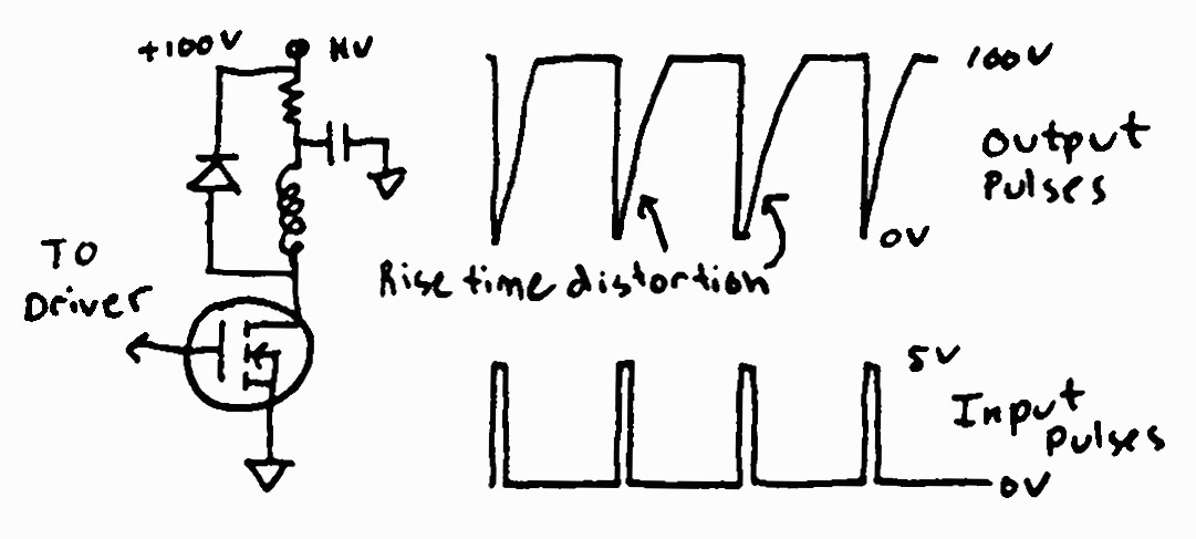
If we go back to our original example of the basic pulse duration modulator described earlier, when the modulator device (switch) opens, the voltage rise is dependent on the energy stored in the input inductor. Any capacitance which exists in the modulator device, filter components, wiring, etc will slow down the rise time of the signal. At high percentages of negative modulation, the on-pulse width is very small and results in very little energy storage within the inductor. Since there is so little energy available to charge the stray capacitance, the rise time of the pulse becomes quite long. This causes the modulation to flatten out, as 100% negative is approached, until the input pulse becomes so small that the driver bandwidth limit causes the input pulses to disappear altogether, at which time the transmitter will suddenly reach 100% negative modulation. Large corporations such as the Harris company have spent much time and effort in trying to solve this problem as has the author of this article. Figure F shows the output pulses, and the pulse distortion.
Several solutions currently exist which will work around this problem. One solution is to use an active pull-up in the modulator. This can be accomplished by using Totem-pole or complementary-symmetry in the modulator output. Another solution is to simply reduce the level of the modulator input pulses, along with the pulse width, so that, as the input pulse width is decreasing, so is the drive level. By the time the input pulses are small enough where the output pulse distortion would be a problem, the tube is operating almost as an analog amplifier, and is cut-off before the input pulses become very small. This is the solution which I used in my KW amplifier. The tube is only operating in the analog domain when the transmitter is near 100% negative modulation, and is handling very little power, so the efficiency of the system is reduced by only a very small amount.
Driver Considerations
If the modulator device(s) are solid state (FET, Transistors, etc), then the pulse amplifier or driver will be only be required to produce a few volts of output. However, since the input capacitance of solid state devices can be very high, the driver must have a low impedance, and be capable of delivering a high peak current in order to charge the input capacitance of the modulator devices quickly, and maintain a good rise and fall time. The pulse generator shown earlier in figure E will drive a solid state MOSFET modulator directly.
If the modulator device is a vacuum tube, then the driver must deliver a high voltage to the grid-,at the peak grid current at which the modulator will be operating. Although the grid of a tube has a fairly low capacitance, a low impedance driver circuit should be used to maintain good rise and fall times of the pulse waveform. It is recommended that an emitter or source follower, or other low output impedance circuit be used ahead of the grid of the modulator tube. If the driver must deliver a varying level to the grid of the tube (recommended to reduce distortion), then the driver must incorporate a good analog amplifier which will control the level of the driver output pulses.
The use of power MOSFETs is recommended over standard bipolar transistors for both solid state modulators and drivers for vacuum tube modulators. The MOSFETs have a very low on-state resistance, are available with higher breakdown voltages than bipolars of similar power, require no gate current (bipolars require base current), and are generally less expensive than similar bipolars. MOSFETs can be driven directly with TTL logic (as shown in the driver example), which greatly simplifies the circuit design.
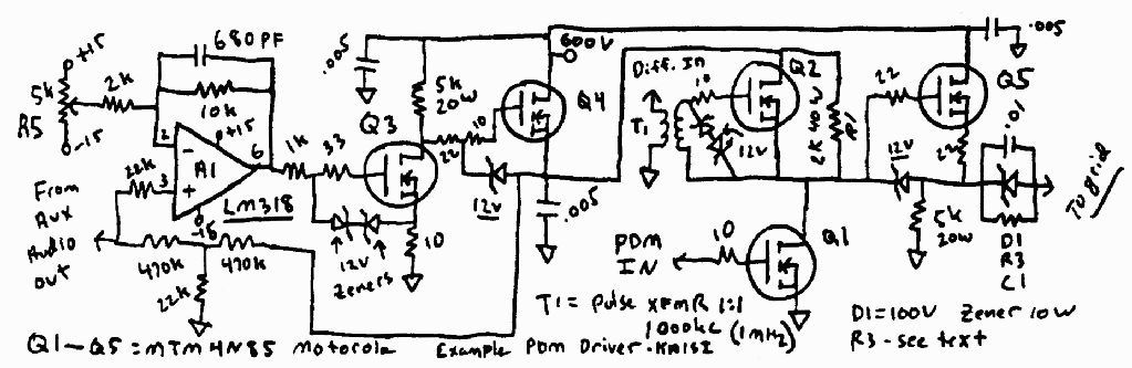
Figure G shows a pulse driver. The driver circuit shown produces varying height pulses up to 600 volts, for driving the grids of pulse modulator tubes. The PDM output from the pulse generator is fed to the gate of Q1, which forms a voltage amplifier with drain resistor R1. Q2 is fed differentiated pulses which occur on the falling edge of the input to Q1. When Q1 turns off, Q2 is turned on, improving the rise time of the output. The pulse amplifier formed by Q1 and Q2 receives power from emitter follower Q4. Q3 and Q4 form an audio voltage amplifier driven by A1. Resistor R5 sets the DC level produced by the voltage amplifier. Audio is fed to A1 from the output of the pulse generator auxiliary audio output. Since the pulse amplifier receives its power from the audio voltage amplifier, the pulse output level is controlled directly by the output of the audio voltage amplifier. This produces varying height, varying width pulses, which depend on the level of audio. The output from the pulse amplifier is fed to source follower Q5, which drives the grid of the modulator tube. A grid leak bias network formed by D1-R3-C1 provides -100Volts bias for the modulator. The value of R3 depends on the grid current of the modulator. If a large enough zener diode, D1, is used, the resistor is not necessary. A 10 Watt Zener was used in this example, so the resistor is necessary to prevent burning out the zener.
Modulator Tube Operating Conditions
There is little data commonly available about operating tubes in pulsed service. However, pulsed service is very similar to class C RF service. The modulator tube should be turned on as hard as possible, to get the highest efficiency possible. To this end, the grid should be driven close to, but not exceeding the maximum grid current or grid input. The screen grid (if used) will have a big effect on the efficiency. It should also be run at fairly high input (not over max ratings, of course!) to get the highest possible efficiency. The average plate current for the tube should not be exceeded, and is recommended that a reasonable safety factor be included. The grid bias required should be just enough to ensure that the tube is completely cut-off when the driver is not delivering an on pulse to the grid. This information can be obtained from curves for the tube. Lacking those, it may also be determined by experiment, once the modulator is operational. Hi-mu tubes make the best modulators, since they require the least amount of grid voltage swing for the greatest output. If a tube requires a lot of grid voltage, it may be very difficult to build a good driver.
Damper Diode
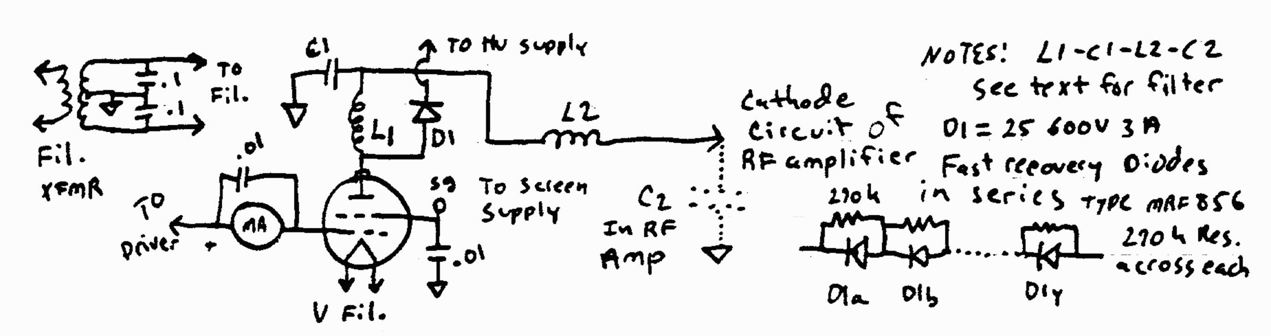
The damper diode conducts the flyback energy developed when the modulator device is turned off back to the power supply, clamping the waveform to produce a good square wave. The diode must switch and recover fast enough so as not to allow "spikes" before the diode turns on, or dissipate large amounts of power when the modulator turns on. There are many fast-recovery solid state diodes on the market which will work in the application. Normal power supply rectifiers are too slow for switching duty, and will burn up excessive amounts of power in switch service. For a high voltage application, it will be necessary to use several solid state diodes in series with equalizing resistors. The cathode of the diode must be well bypassed to the modulator chassis so ensure a good clean switch of the rising edge of the wave, as the damper begins to conduct. This energy is, of course, returned to the power supply. The damper diode is handling a considerable amount of power, and should be chosen with this in mind. I used a string of 25 600V 3A fast recovery diodes with 270K 1w resistors across each diode for equalizing. Note: DO NOT use mercury vapor rectifiers, gas tubes, or standard power supply solid state rectifiers for the damper diode!! These devices are too slow for the application, and will most likely burn up or arc over in the application.
Output filter construction
The construction of-the output filter is very important. One of the biggest problems encountered in filters of this type is ringing. Any ringing in the switching waveform will cause distortion of the modulated signal. Another problem is self resonance in the inductive elements. Once a filter is constructed, and the modulator completed, the waveform occurring at the input to the filter must be checked over the entire range of pulse widths to ensure that no ringing, waveform distortion or other anomalies which will cause distortion.
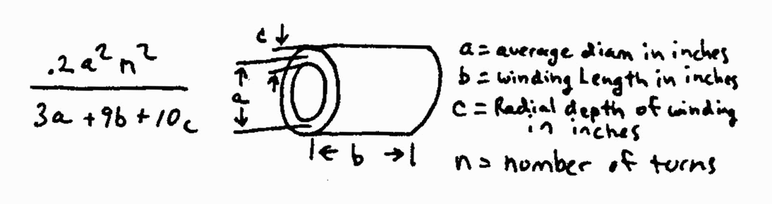
The best kind of inductor I have found for use in these filters, at least for the input inductor is an air-wound RF choke. For modulators designed to modulate RF amplifiers with an impedance of around 8000 ohms, values in the range of 40mH to 70mH are typical. These are fairly large inductors. The choke has to be able to withstand the full power supply voltage (in my case, 10000V) across it, and be able to carry the full peak current under maximum modulation. It should also have low resistance, since you don't want to burn up too much power in the choke!
A 40mH inductor air-wound inductor can be wound on a 4 inch form (I use 4 inch PVC pipe), 5 inches long, with around 600 turns. A rough estimate of the inductance can be calculated using the following formula:
Click here for graphic of formula
I used #22 gauge enameled wire to make the chokes. The chokes are wound in layers. Each layer is wound in a criss-cross fashion to minimize any resonances. Between each layer of wire are 6 layers of waxed paper. I started off with 20 turns per layer for about the first 10 layers or so, then dropped to 15 turns per layer for the next 12 or so layers, then went to 9 turns per layer for about 15 layers, then 6 turns per layer for 10 more, then finally just 3 turns for the last 5 layers.
THIS DATA IS APPROXIMATE! The number of turns, and the number of layers depends on the value of inductance you need, and the voltage that the choke has to withstand. Don't be intimidated by the construction of the choke. I’ve made 5 of them so far. Once you get the hang of it, you can make one in about 4 hours.
The capacitors used in the output filter should be of good quality, and rated at least as high as the power supply voltage.
Building the Modulator
Although the modulator section (following the pulse driver) is fairly simple, there are some conditions which must be analyzed. Since the modulator is handling RF frequencies (the switching waveform), with very fast rise and fall times and high harmonic content, the cathode of the modulator (if a tube), and all other leads leaving the modulator cabinet should be suitably bypassed to prevent generation of BCI and TVI. If the cathode is not bypassed with a low reactance at the switching frequency, the inductance of the filament transformer will isolate the cathode from true ground, and may cause unpredictable results in the modulator.
The collector, drain, or plate circuit of the modulator must not introduce any more stray capacitance to ground than necessary if good rise and fall times of the pulses are to be maintained. To this end, the filter should occupy the same enclosure as the modulator, with a direct, unshielded, unbypassed line going from the modulator to the first filter element. The remainder of the filter need not be located near the first reactor, since there is a relatively large capacitance following the first reactor, although it may be convenient to keep the whole filter in one location. Figure H shows the modulator, filter, and damper diode as part of a PDM transmitter.
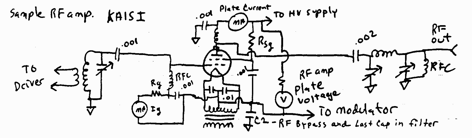
The RF amplifier
Up to now, there has been little discussion of the RF amplifier. The RF amplifier is a standard class C amplifier which is designed to allow a varying DC voltage to be imposed on the negative side (cathode side). and a fixed DC voltage on the positive side (plate side). The DC paths for the grid and cathode circuits must float above ground, while the RF paths are referenced (and bypassed) directly to RF ground (chassis) as in a normal RF stage. It is not necessary to float the entire grid circuit above ground, and the RF may be coupled to the grid through a high voltage capacitor or RF transformer, allowing the use of normal grid components, so long as the DC path does float along with, and is referenced to the cathode.
It is highly recommended that the last capacitor in the PDM filter be used to bypass the cathode of the RF amplifier to ground, as part of the RF amplifier. This will result in the most stable RF design, while still maintaining the proper value for the filter. A capacitor with a low series inductance should be used. All other grid RF bypasses and references such as the grid leak resistor, screen bypasses, suppresser, etc must be connected to the cathode, so, as the cathode voltage varies with respect to the plate, the control grid voltage is NOT varying with respect to the cathode.
If a screen resistor is used, in the case of a tetrode or pentode, the resistor is simply connected directly to the DC plate supply. All circuit components with the exception of the filament transformer, which must withstand the full power supply voltage under 100% negative modulation, are the same as a standard dc-grounded cathode, class C RF amplifier. Figure I shows a representative RF amplifier, used in a PDM transmitter.
Power Supply
The power supply in a PDM transmitter must supply the full voltage required to modulate the RF amplifier to whatever positive modulation is desired. If you want to run 3000Vdc on your RF amplifier, and you want to be able to modulate the RF stage to 150% modulation, then the power supply must deliver 7500Vdc. The current that the supply must deliver is related to the RF amplifier power input, ratio of total power supply voltage to RF amplifier voltage, and the efficiency of the modulator. As an example, let's say the RF stage runs at 2000V at .2A (400W) total power input. All powers (screen input, etc) which pass through the modulator must be added together to get the TOTAL power input. The transmitter is to have a positive modulation capability of 150%, so a 5000V power supply will be used. The modulator efficiency is 90%. We can calculate the total power input to the system by dividing the power input to the RF amplifier by the modulator efficiency. This is aprox. 444.5 watts. Since the power supply delivers 5000V, the current required for 444.5 watts is approximately .089A. For carrier conditions, the supply must deliver 5000V at .089A. Under 100% modulation the power input will be 50% (the energy in the sidebands) greater than the carrier level, or around .135A under 100% sine wave modulation.
Metering a PDM transmitter
Meters should be permanently connected to the following circuits in a PDM transmitter for the purpose of monitoring operation and adjustment:
Modulator: Control Grid current
| Screen current (if applicable) |
RF Amplifier: Plate Voltage (measured from cathode to plate)
| Grid Current | |
| Screen Current (if applicable) | |
| Plate Current |
Power Supply: Total Power Supply Current
| Power Supply Voltage |
Since many of the circuits which require metering are floating at the full power supply voltage, the meters should be recessed behind glass or other clear, insulated panels, to prevent voltage breakdown to ground, and danger to operators and visitors.
Testing your new PDM transmitter
Each part of the transmitter should be fully tested as it is built, if possible. All the low level circuitry should be fully operational and tested, up to the grid of the modulator tube before any operation is attempted. It is highly recommended that the waveforms at various key points in the transmitter be measured and recorded for future reference. The output of the driver should be checked with the modulator grid connected, operating at the correct grid current. Remember, the modulator grid current will be considerably higher when there is no plate voltage applied to the modulator, than in actual operation. The whole range of pulse widths should be checked to make sure that rise and fall times are not too long, and that there are no sudden changes in pulse width, oscillations, or other unusual occurrences which will cause serious distortion.
The RF amplifier should be tuned up at reduced power supply voltage, with the cathode circuit temporarily grounded. Once this is set up properly, then the modulator will be working into the correct load, and can be checked out properly. A suitable high voltage probe should be used to check the output of the modulator, at the input to the filter. It is not necessary to operate the modulator at full voltage, but the proper load resistance must be presented to the output of the filter, or waveform distortion may result. The output switching waveform must be free from tilt, ringing, or other abnormalities. An improper waveform will result in SERIOUS distortion.
If your modulator incorporates a driver which adjusts the drive level with pulse width, this adjustment should be made before attempting to actually use your modulator. It is necessary to feed a sine-wave signal into the input of the modulator, and observe the modulation envelope on an oscilloscope. A 1000Hz tone should be a good frequency to use for this adjustment. First, reduce the analog level to 0 (or its lowest value) and bring up the modulation level. You will notice that at some point, the modulation will jump from some finite value (probably around 90%) to 100%, and will be observable on the scope. Back off the input to the point just before the jump to 100% negative is observed. Now, bring up the analog (drive compensation) level until the transmitter is 100% modulated. The modulation should be clean, and the sine wave should be rounded and undistorted. If not, do some checking! Something is probably wrong.
Run the oscillator through the whole audio range to make sure the transmitter has a flat response, and there are no resonances or other problems anywhere in the range the transmitter is designed to operate. Try bringing the oscillator up to a very high frequency to verify that the input filter is working, and that aliasing is not objectionable.
Adjust the negative peak limiter (if included) to the desired level (95% is a good place to clip it), but don't use too much... you have a good transmitter... and clipping is distortion although it is recommended that the clipper be enabled - just as an insurance against overmodulation. Of course, if conditions are bad, or there's a lot of noise, it's always nice to 'crank up the audio' and not worry about overmodulating, or blowing up a modulation transformer!
A final check should be made of the switching frequency level. Using a local receiver, or a friend who has a good receiver, and is close by, check the level of the sidebands produced by the switching frequency, on the upper and lower side of your carrier. They should be down 70dB or more from the carrier (if you designed your filter properly!).
Please keep in mind, that the pulse duration modulator system described here is just one implementation. There are many other ways to achieve the same result, with a completely different configuration. Although commercial firms are doing some research in the area of improvements and other implementations, the Amateur community can do much to further the state of the art in this area. The more advances we make, the more ammo we have for the FCC, when we ask for a special provision for the AM power limit... why, just look at these technical advances we're making...Surely this serves the public interest...
NORTHEAST AM SCENE
by Bill Wolf - KA2EEV
ELBOW ROOM DEPARTMENT: Everyone knows where to listen for AM signals because of a phenomenal evolution over the years. Traditional places on the dial formed by creatures of habit. What's that you say? You still can't dislodge that 25 years of hardened chewing gum from your dial? Seems to me that we need to exercise more flexibility with our "AM windows", particularly in regard to 75 meters (3860 thru 3890 KHz) since 75 always rates highest with continuous activity and number of AM stations. There always seems to be a natural tendency, however, for us to tune within a specific 10 kc segment (need I mention frequency?) where several AMers usually align themselves for a scrunched in QSO when there is often a reasonably open frequency lower down the band. What really floors me is when another fellow AMer either starts testing or calls CQ within 2 or 3 kc of an existing AM QSO! Thankfully there's only a select few such morons whose table manners lend a convincing link to Darwin's theory. Anyway, it would be great to see more AMers claim "territorial rights" down near 3860 or even 3850 during regular peak hours. Aside from providing extra elbow room it would also send a message to sidebanders that they can expect to encounter annoying heterodynes from AM carriers whenever they choose to enter our turf. Suggestion then ... the next time you find yourself engulfed within a flock of sheep, especially one of those large round tables, give one of your AM neighbors a friendly nudge with an invitation to QSY.
EAST COAST SOUND DEPARTMENT: Is it live or is it AM??? If someone should tell you that your rig has that "east coast sound", relax and smile, they're paying you an extraordinary compliment! It's something which every Johnny Novice dreams of (besides getting that special date for the prom). Having the east coast sound is tantamount to saying that your audio has exceptionably good frequency response. You’re likely to be especially proud, and rightly so, if someone pays this compliment to your modified Valiant or Apache since these two rigs are notorious for restricted stock audio. I might sooner listen to one of Arthur Godfrey's old 78's than hear a stock Valiant.
SPRING, TEXAS DEPARTMENT: I just can't help from mentioning Otis, K5SWK, of Spring, Texas, whose signal here in the northeast was notably strong during late February and early March on 75 meters. Otis, by the way, has a keen sense of humor and he happens to be one of those Texans with the east coast sound. If you are fortunate enough to work K5SWK and if you listen carefully... you just might hear his old dog "Sarge" in the background. (See AM Press Exchange, issue 38, Aug. ‘86, page 9, for exclusive photo).
Eat your heart out Spuds MacKenzie!!!
SPAM REPORT
RESULTS: End of January 75&160M AM JAM-BO-REE!:
This year's 75(&160 combined) AM jAM-Bo-Ree was the biggest ever! More stations reporting higher scores than before. Although we have received a lot of mail saying we should go back to single band events, this year's "experiment" with a Thanksgiving ALLBAND and a combined 75&160 event was successful. Scheduling may permit a return to single band events next year. As could be expected by a listener to this event, W8VYZ, Ashtabula Bill was on continuously and as a result tallied up the highest number of points - A RECORD I THINK- 1,716 !! So congrats are in order for that perseverance, Bill! But these are not CONTESTS & ALL who participate enjoy contacting new friends on AM. K8MLV/0 next closest in numbers got 1300 points and said "I spent too much of my operating time on 160 -could have done better." Well done, Rick! Dale, KW1I still prefers the single band events, but did very well - 1,122 points. YET ANOTHER SCORE OVER 1000-Walt, KJ4KV with his T-195 (100 watts!) Walt has high praise again for Bill(VYZ). Dale and other "big guns" and regulars that kept things going and kept the AM windows "open" hi. Walt's log shows new AMers AND he even had the opportunity to introduce a YL to AM . Bob in Glastonbury, CT WB1GCM is our next highest counted scorer with a whopping 850 points. But Bob deserves praise also for his taking the opportunity to earn SPAM membership by working the jAMboree. We hope others will. do likewise! Next is the well known Ozona Bob, W5PYT who turned in logs for 75 and 160m jAMboree activity. He worked a lot of stations on both bands for a total score of 792 . Outstanding Bob! Bob says Sunday night was better for him. Others may have done better Saturday evening. Depended on what part of the Country you were in I guess. Another well known AMer Is Dick, W2UJR , with another "vote" for single band events, but pts in this one were quite good- 494 ! He says they have a big group on every morning 6-7:30 EST on 1888 . Not far behind that is Fred, W5JKD from Priddy, TX -our SPAM logo artist. By the time you read this, I HOPE we will have SPAM stationery with that logo on it. Fred got about the same number of contacts on 160 as he did on 75, for a total of 468 points. VY. GOOD! ANOTHER NEW SPAM MEMBER is Bill from the Boulder (Lyons) CO. area - KD0HG . Bill is one of those that worked a "rare" one - WA5TWF, hi . His fine score is: 360 pts. Hardworking State Director for Maine, NE1S, Larry, had fun and turned in a vy. good score of 352 pts. W6HDU (Doing a good job of representing the West) Sam got 319 points using his newly operational KW1. Sam called SPAM Hq about 6 weeks before the jAMboree and I'm pleased I could assist him because he is doing vy. FB on many bands with that rig. We need such "big signals" from out there and am vy. pleased that we have West Coast stations appearing on the logs for this event. Ralph, K4HOL, was "not out to break any records, but had some nice contacts with AM.ers". Hey! That's "what it’s about!" His score is a very fine 190 points. From WAY UP THERE IN CANADA, we have VE1CDT reporting 144 points. Harry had fun, and got more contacts than previous because his line noise went away. Paul, W3HHC, is celebrating 50 years as a ham op. He didn't have much time but did get that "rare one" (SPAM HQ). Jerry, WA4KJK only had 50 minutes to operate this jAMboree but got a good score of 104 points. With DX-100 and 75A4 he now has a "100% 50s era set-up" and a $3. fleamarket typewriter too hi (works good). In the "Ranger Class" we have W7JKY (Oregon!). Barry worked a lot of 5s but there were some 6s I had not heard - Barry did fine with 75 points. Tied with 75 pts also is "Dallas John" - he worked a lot of stations (but mostly Texas) not bad at all for low power . John had a lot of work that interfered with his operating time, too. With the "true spirit of ham radio" is Bob in N.J. W2HBE- Super low power - 35w input to an 807& Marconi ant 27' abv. gnd. on 160m ONLY, turning in a 63 point score. VY GOOD! Ed, W8JYY, in Ohio is enjoying his first operation on AM for many years- and it is FUN! Worked 160m ONLY for a point total of 35. ALL these AMers are WINNERS!
- 73 de WA5TWF
EXCHANGE
(Names omitted - Past Copy)
TRADE: Have Collins 32V2. Will trade for Colt 1911A1.
WANTED: Johnson Ranger manual desperately needed. Will buy original or a GOOD photocopy.
FOR SALE: 833-A triode, unknown condx. but looks decent shape, $10.
WANTED: Parts for Hammarlund HQ160, HQ145 or HQ110 receiver. Also need finals for Globe Champion 300A - Amperex 6083/AX9909.
FOR SALE: SX-96 $100; SX101 MKIII $125; SX117 $110. All with manuals. Excellent shape. Call collect on parts only.
WANTED: Interstage audio transformers, HI-FI output transformers.
FOR SALE: Collins KW-1 beautiful condition s/n 141 serious offers. KWS-1, 75A4 mint condx $1000 or best offer. 75A3 excellent condx $200. HT-32B mint condx $200. Ranger I excellent condx $100. Local pickup or you ship.
FOR SALE: Hammarlund HQ170A $150 mint. Heavy duty 400 ma. filter chokes $20 ea. Oil capacitors 10 mfd @ 7.5 Kv $30 ea. 4 MFD @ 10 KV $40 ea. 805 transmitting tubes $20 ea. 810's $20 ea. 100TH $15 ea. 813 $20 ea. New octals and loctals $2 ea. 7 & 9 pin miniatures $1 ea.
WANTED: UTC LS-49, Chicago BD-2 30-watt audio transformers.
Part 97 Rewrite - An Editorial
GOING TO DAYTON? Fred Maia, W5YI (W5YI Newsletter) plans to have copies of the new rules ready for distribution at the Dayton HamVention (Booth 475). We strongly urge all AM'ers who plan to attend to pick up copies of the proposal, and to attend the FCC Forum, where Johnston is scheduled to address the HamVention.
The AM community is urged to carefully read this proposal, including all the fine print, being alert for any proposed changes which would adversely affect AM operation. Remember, it was John B. Johnston who unveiled the infamous Docket 20777 at the FCC Forum at Dayton in April, 1976. Hailed as "deregulation", Docket 20777 proposed to outlaw all AM operation below 28 mhz, by deleting specific emission designators from the rules, and limiting all signals to SSB bandwidth.
We should be especially concerned over the proposed changes in emission designators under the latest proposal, PR Docket 88-139. For those of us who participated in the opposition to Docket 20777, what we have heard so far has a disconcertingly familiar ring to it. The reported proposal to delete specific voice emission designators and to incorporate them all under a reference to "phone" sounds suspiciously similar to what was proposed under Docket 20777. This idea raises many questions. For example, how will the rules distinguish between wideband FM, permitted above 29.0 mhz, and the more narrow-band voice modes currently in use on the lower frequency bands? How will the FCC maintain its SSB-only clause in the 10 m. Novice phone band? Will specific bandwidth limits be imposed? At this time there is insufficient information available on which to draw any firm conclusions about what is being proposed. The ARRL Letter suggests that ARRL will support the overall effort to reorganize Part 97, but that the League will be taking exception to some of the substantive changes being proposed.
AM'ERS ATTENDING DAYTON are STRONGLY urged to attend the FCC Forum. At the question-and-answer session which follows Johnston's speech, we must impress Johnston and other FCC officials that there is indeed substantial interest in AM in the Amateur community - by fielding intelligent sounding questions SPECIFICALLY ADDRESSING the AM issue.